Z3816A Output Modification
This page describes a modification I made to convert the 19.6608 MHz outputs to additional 10 MHz outputs.
Introduction
The Z3816A is a GPS disiplined timing source that was manufactured by HP in the middle 90's. It was intended for use in cellular telephone equipment. It provides 10 output signals through sma connectors on the back panel.
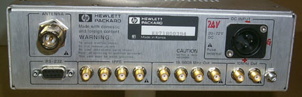
Output Signals
- 1 PPS -- from the 4 connectors on the left. This is signal is based at 0 V. Every second a 4 V positive-going square pulse into 50 ohms (5V open circuit), 20 uS wide is generated.
- 19.6608 MHz -- from the next 4 connectors. This is a square wave signal between 0 and 4 V into 50 ohms (5V open circuit).
- 10 MHz -- from the two connectors on the right. This is a 3.2 V p-p sinewave into 50 ohms (6.3v p-p open circuit).
The 19.6608 MHz signals are easily divided down to decimal fractions of a second or into standard baud rates. For my purposes, I planned to use the Z3816A mainly to generate time bases for test equipment. The 10 MHz signals are useful for that purpose, but the 19.6608 MHz signals are not directly helpful.
I decided to see if I could figure out a way to modify the Z3816A to convert the 19.6608 MHz outputs to additional 10 MHz outputs. I assumed these four connectors would need to remain as square wave outputs, but that is ok.
Opening the Z3816A
To try to figure out part of the circuity, I had to disassemble the Z3816 and remove the circuit boards.
This requires torx screwdrivers.
Here are the basic steps:
- Remove the top cover.
- Remove the screws and brackets mounting the power supply board. Unplug the cables and remove the power supply board.
- Remove or loosen the front panel. Remove the four screws. Loosen the nut on the main power switch. If this nut is left attached but very loose, the panel can be pulled off of the LED's and rotated. If the power switch nut is removed, the front panel can be completely removed.
- Remove the main board. Unplug the antenna wire from the main board. Remove all the nuts on the sma connectors on the back panel. Remove all the torx screws holding the main board and lift it out.
Disclaimer
When looking at the main board, I found that there are a few wire jumpers applied to the board. As we will see later, two of these jumpers are right in the area that I ended up modifying. I don't know if most Z3816's will have this same factory rework. If you want to apply this modification to another unit that does not have the same factory rework, you may have to do your own snooping to see how your circuits are wired and adjust the modification.
Looking at the board
Here is a picture of the interesting portion of the top of the main board.
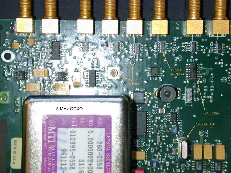
Some of the results of sniffing around with a scope and continuity tracer are shown in the labels. In the bottom-right you can see that there is a 19.6608 MHz crystal. This is apparently the source of the 19.6608 MHz output. I assume that this must be locked somehow to the basic 5 MHz OCXO which is locked via the GPS satellite signals. I never found how this locking of the 19.6608 MHz might happen though. If anyone knows more, I'd like to hear about it.
The (74)F74 chip in the upper right seems to take the 19.6608 MHz signal and gate (or otherwise generate) the 1 PPS signal that drives the four 1 PPS outputs. It can be seen that there are two factory jumper wires in the area of this chip.
The 10 MHz signals seem to be generated in the upper left corner of the picture. The labels show two of the key test points that provide 10 MHz signals. The small coax connector (J5) near the top center provides a square wave 10 MHz, but the TP14 seems to be one of the earliest and cleanest 10 MHz signals. The 14-pin chip to the left of J5 is a 74ACT04 that distributes versions of 10 MHz.
There is a resistor pack (labeled Output R-Pack in the image) for each of the square wave outputs of 19.6608 and 1 PPS. More details on these circuits later.
Here is a picture of part of the bottom of the main board.
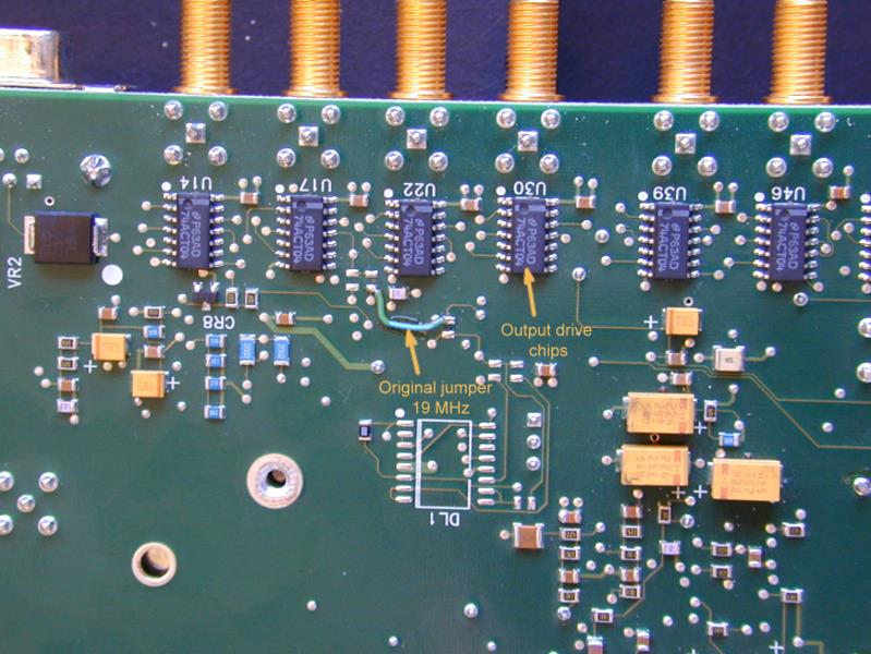
Each of the eight square wave outputs ( 4 - 19.6608 MHz and 4 - 1 PPS) has a 74ACT04 buffer chip as seen across the top of the image. Each of these chips provides the drive for one of the square wave output signals. More on these circuits is described later.
The factory jumper wire, shown slightly to the left of center in the image, turns out to be part of the distribution of the 19.6608 MHz signal. The left side of the wire is connected to the source of 19 MHz. The right side of the wire connects to a net that feeds each of the 19.6608 MHz output buffers, but also feeds the input to the F74 chip that is needed for 1 PPS output generation.
Here is the circuit for one of the outputs.
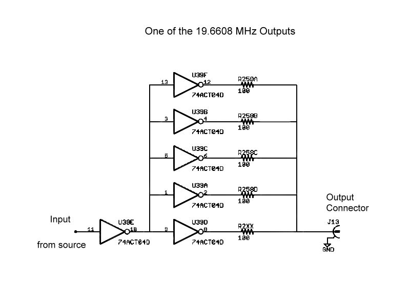
The same general circuit seems to be used for each of the square wave outputs of 19.6608 MHz and 1 PPS. A single 74ACT04 chip drives each of the outputs. The R-pack chips provide the 4 resistors in the top of the schematic and the bottom resistor is provided by a single SMT resistor. The four 19 MHz drivers have their input from a common net, and the four 1 PPS drivers have their inputs from a different common net.
Modifications for more 10 MHz outputs
Here are the steps I took to make the modification.
- On the bottom of the board, remove the one factory jumper shown in this image.
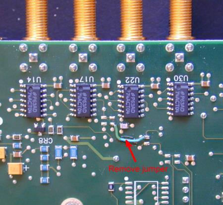
This isolates the 19 MHz source from the output net. The output net also feeds the F74 chip, so this will need another step.
- Remove the factory jumper that feeds U31-pin3 and add a new jumper from pin3 to a near-by via.
This is shown the image below.
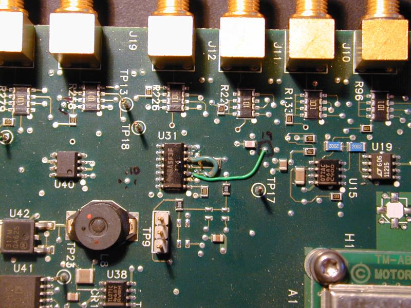
Removing the factory jumper isolates U31-pin3 and the new jumper feeds it 19.6608 MHz from a different source net.
- Add a new jumper from TP14 to the via near R279 as show in this image.
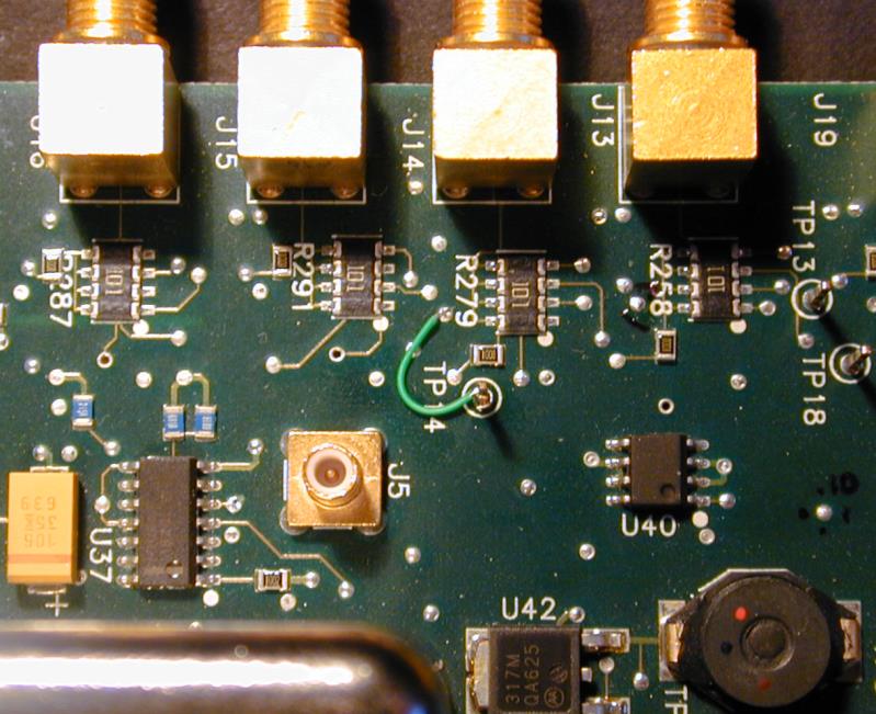
This connects the isolated net that feeds the four 19.6608 MHz drivers with a source of 10MHz signal.
That's it. The four outputs that were 19.6608 MHz should now be a 10 MHz square wave. The four 1 PPS outputs should still work. I tested mine before reassembling everything by putting the main board and power supply board on an insulated bench. I plugged the power supply board and the main board together with their cable. I then provided 24 VDC to the two input pins of the power supply board. The alarm signal will light without any GPS antenna connected, but all the output signals should be present to confirm proper operation.